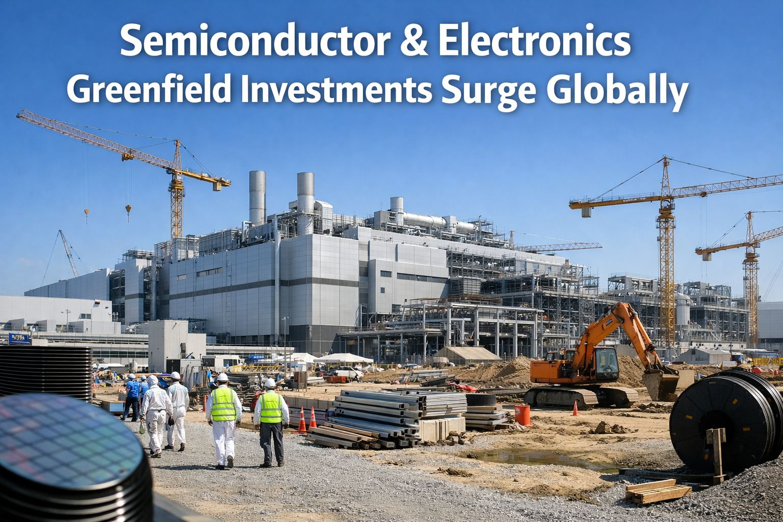
Global semiconductor sales hit $791.7 billion in 2025 — up 25.6% year-over-year — and are projected to breach $1 trillion in 2026. Behind these record numbers is something unprecedented: the largest wave of greenfield fab construction in the industry's history. Over 170 new chip facility investments were announced in 2025 alone, driven by AI demand, geopolitical supply chain restructuring, and $280 billion in government incentives from the U.S. CHIPS Act alone. For manufacturers, equipment suppliers, and facility planners, this isn't just a market trend — it's a generational buildout that will define industrial geography for decades.
Planning a semiconductor or electronics greenfield facility? Book a free 30-minute consultation to see how iFactory embeds AI-powered maintenance, cleanroom asset management, and predictive intelligence into your plant from the design phase.
Why Semiconductor Greenfield Investment Is Surging
The semiconductor industry is experiencing a construction supercycle unlike anything in its 70-year history. Three converging forces are driving companies and governments to build new fabrication facilities at an unprecedented pace — reshaping global supply chains and creating enormous demand for smart plant design, advanced maintenance systems, and operational technology.
The AI Infrastructure Boom
AI chips now drive roughly 50% of industry revenue despite representing less than 0.2% of total chip volume. Logic product sales surged 39.9% in 2025 to $301.9 billion, while memory products — critical for AI accelerators — grew 34.8% to $223.1 billion. This extreme concentration of value in AI-related chips is pulling massive capital investment into new fabs optimized for leading-edge logic and high-bandwidth memory production.
Geopolitical Supply Chain Restructuring
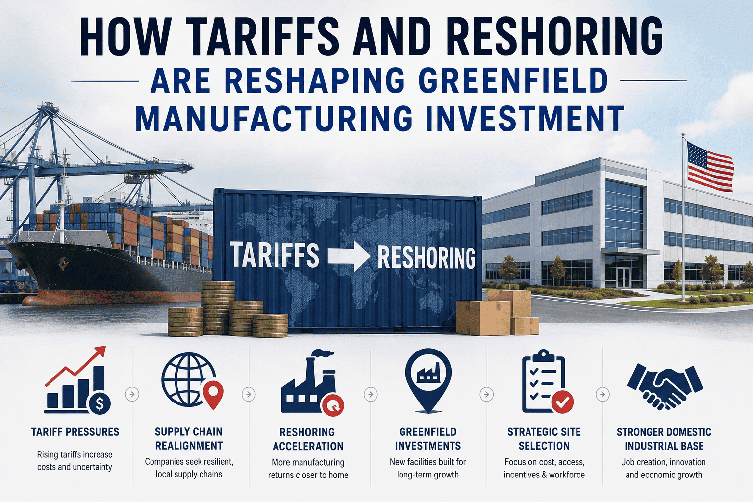
The geopolitical distance of greenfield FDI announcements has dropped over 20% since 2010, as companies increasingly invest closer to geopolitical allies. Foreign semiconductor investment into mainland China has collapsed to roughly 20% of its 2015–2019 average — an 80% drop in dollar terms. Capital is flowing instead to the U.S., Europe, Japan, India, and Southeast Asia as companies pursue "de-risking" and "China+1" diversification strategies.
Government Industrial Policy & Incentives
A global wave of semiconductor incentive programs — led by the U.S. CHIPS Act ($280 billion authorized), the EU Chips Act, Japan's subsidy programs, India's Semiconductor Mission, and South Korea's tax incentives — has created the most favorable policy environment for fab construction in decades. The U.S. alone has awarded $30.9 billion in direct funding to 19 companies for 40 projects as of mid-2025.
The Scale of the Buildout: By the Numbers
The numbers behind the current semiconductor greenfield wave are staggering. Here's a snapshot of the investment scale, capacity expansion, and market forces driving the largest industrial construction program of the 21st century.
Global Chips Acts: The Policy Landscape
Government incentive programs are fundamentally reshaping where semiconductors are manufactured. Every major economy now has an industrial policy targeting chip production — creating a competitive landscape where facility location decisions are driven as much by policy incentives as by market fundamentals.
$39 billion in manufacturing grants, 25% investment tax credit, and $11 billion for R&D. As of mid-2025, $30.9 billion awarded to 19 companies for 40 projects. TSMC has committed $165 billion total investment in Arizona fabs. U.S. capacity projected to reach 203% growth by 2032.
Five pilot lines launched in early 2025 targeting 2nm and advanced packaging. Germany confirmed €1 billion support for Infineon's €5B fab expansion in Dresden. EU approved €450M for onsemi's SiC power devices fab in the Czech Republic.
Four additional fabs approved in 2025, including SicSem's wafer fab in Odisha. India Semiconductor Mission aligned with IndiaAI initiative deploying 34,000+ GPUs. India ranked as the third-largest recipient of greenfield FDI projects globally.
Tax credits ranging from 16% to 35% for semiconductor investments. Government targeting 50% domestic sourcing of manufacturing materials by 2030. $900 million allocated for AI chip technology development through 2026.
Major subsidies supporting TSMC's Kumamoto fab, Rapidus's 2nm facility targeting mass production in 2027, and Samsung's advanced packaging operations. Japan positioning as a critical node in the allied semiconductor supply chain.
Vietnam targeting 100 chip design firms by 2030. Malaysia's National Semiconductor Strategy scaling assembly and test capacity. Singapore leading in AI governance and data center infrastructure. The region receives 2.5x its fair share of global semiconductor FDI.
Building a Semiconductor or Electronics Facility?
iFactory's AI-powered CMMS integrates into your greenfield project from the design phase — ensuring your maintenance strategy, cleanroom asset management, and equipment intelligence are operational before first wafer.
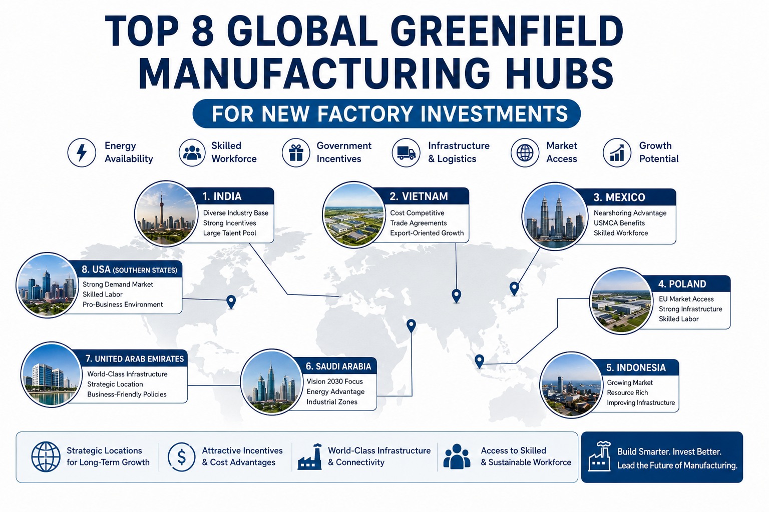
The New Semiconductor Geography: Where Fabs Are Being Built
The global semiconductor supply chain is being fundamentally rewired. Investment that once flowed overwhelmingly into East Asia is now distributing across a wider network of allied nations — creating new manufacturing corridors and reshaping the industrial geography of chipmaking for decades to come.
What Makes Semiconductor Greenfields Different
A semiconductor fab is among the most complex and capital-intensive facilities ever built. The design, construction, and operational requirements are fundamentally different from any other type of manufacturing plant — and the margin for error is essentially zero.
Extreme Precision Environments
Cleanrooms must maintain ISO Class 1–5 standards, with particle counts measured in parts per cubic meter. Temperature, humidity, and vibration must be controlled to nanometer tolerances. A single contamination event can destroy an entire wafer lot worth millions.
Massive Power & Utility Demands
A modern fab consumes 100+ MW of continuous power — equivalent to a small city. Ultra-pure water systems, chemical delivery, exhaust abatement, and backup power generation must all be designed and commissioned as integrated systems.
Multi-Billion Dollar Equipment
A single EUV lithography machine costs $350+ million. A leading-edge fab contains thousands of precision tools, each requiring specific maintenance protocols, vibration isolation, and environmental controls. Equipment uptime directly determines fab output and revenue.
Years-Long Construction Timelines
From groundbreaking to first silicon, a leading-edge fab takes 3–5 years and costs $15–30 billion. Every month of delay represents millions in lost revenue and competitive positioning. Maintenance and operational systems must be planned years before production begins.
5 Critical Success Factors for Semiconductor Greenfields
With billions of dollars and years of planning at stake, the difference between a successful fab launch and a costly delay often comes down to how well operational systems are integrated from the earliest design stages.
Predictive Maintenance from Day One
AI-powered predictive maintenance must be operational during commissioning — not bolted on months after production starts. Baseline equipment signatures for compressors, HVAC, pumps, and process tools should be established during installation, enabling anomaly detection before the first production wafer is loaded.
Cleanroom Asset Hierarchy Design
Every piece of equipment in a fab — from lithography tools to gas delivery systems — must be mapped into an asset hierarchy that reflects its criticality, maintenance requirements, and interdependencies. This architecture drives work order automation, spare parts planning, and compliance documentation.
Utility & Facility Systems Integration
Ultra-pure water, chemical delivery, exhaust abatement, and HVAC systems are as critical as process tools. IoT sensor networks must monitor these systems continuously, with automated alerts for any parameter deviation that could compromise cleanroom integrity or production quality.
Regulatory & Compliance Readiness
Semiconductor fabs face environmental regulations (chemical handling, emissions, water usage), safety requirements (hazardous materials, electrical), and industry standards (SEMI S2/S8, ISO 14644). Compliance documentation must be built into the CMMS from the design phase.
Workforce Readiness & Knowledge Systems
The semiconductor workforce gap is acute — every major fab project is competing for the same pool of skilled technicians and engineers. Digital work order systems, maintenance procedures, and AI-assisted troubleshooting help new teams ramp faster and maintain quality standards from the start.
How iFactory Powers Semiconductor & Electronics Greenfields
iFactory's AI-powered CMMS is designed to integrate into the most demanding greenfield environments — from leading-edge semiconductor fabs to advanced electronics assembly facilities. Here's how iFactory supports every phase of your project.
Asset Architecture & Cleanroom Planning
Model your process tools, utility systems, and facility equipment with maintenance strategies tailored to semiconductor-grade requirements — including cleanroom-specific protocols, vibration-sensitive equipment, and chemical delivery systems.
Sensor & Telemetry Pre-Configuration
Pre-configure IoT sensor flows for environmental monitoring, equipment telemetry, and utility system performance so your CMMS captures operational data the moment systems are energized — zero gap between commissioning and intelligence.
Predictive AI Baseline Learning
AI models learn baseline signatures for every critical asset during tool installation and qualification — from lithography systems to HVAC compressors — detecting anomalies and predicting failures before they impact yield or uptime.
Continuous Intelligence & Compliance
Real-time dashboards track equipment health, utility system performance, energy consumption, and environmental compliance — supporting yield optimization, audit readiness, and predictive maintenance across your entire facility.
Why Start CMMS in the Greenfield Phase?
In semiconductor manufacturing, every hour of unplanned downtime can cost $100,000 or more in lost production. Deploying iFactory during the design phase ensures your asset hierarchies, maintenance strategies, sensor configurations, and predictive models are fully operational before the first wafer enters the fab — not months later when yield losses have already accumulated and compliance gaps have appeared on audit reports.
Design Your Semiconductor Facility for Maximum Uptime
See how iFactory integrates AI-powered maintenance, cleanroom asset management, and compliance-ready operations into your greenfield timeline — from design through high-volume production.