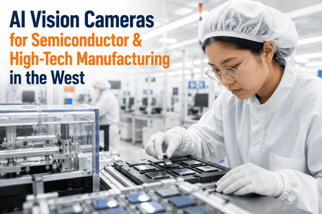
West Coast semiconductor and high-tech manufacturing facilities operate at a precision threshold where a single undetected micro-defect on a wafer can cascade into millions of dollars in yield loss before the process deviation is even identified. From the advanced logic fabs expanding across California and Oregon to the PCB assembly lines driving Silicon Valley's supply chain, the margin for visual inspection error is effectively zero — yet human inspection misses 20 to 30% of defects under real production conditions, with accuracy degrading measurably within hours of a shift. The semiconductor defect inspection equipment market reached $11 billion globally in 2024 and is forecast to nearly double by 2032, driven precisely by this gap: the inability of traditional inspection to keep pace with shrinking node geometries, rising production volumes, and the zero-defect quality standards that advanced chip customers now demand as a baseline. iFactory's AI Vision Camera platform is purpose-built for semiconductor and high-tech manufacturing environments on the US West Coast — delivering real-time micro-defect detection, automated anomaly classification, and yield intelligence that connects directly to production scheduling and process control workflows.
Why Semiconductor and High-Tech Manufacturers on the West Coast Cannot Rely on Traditional Inspection
The Structural Failure of Human Visual Inspection at Advanced Node Production Volumes
Semiconductor fabrication lines in California, Oregon, and Washington are producing chips at node geometries — 7nm, 5nm, and below — where defects smaller than 20 nanometers determine whether a die ships or gets scrapped. At these dimensions, the defect types that destroy yield are invisible to the human eye and detectable only by high-resolution optical, e-beam, or AI-augmented camera systems operating with sub-micron precision. Traditional quality control that relies on sampling inspection intervals, manual operator review at light tables, or legacy rule-based automatic optical inspection (AOI) systems was designed for defect categories and node sizes that no longer represent the majority of West Coast production output. The problem compounds at scale: a modern fab running 24/7 across multiple product families generates inspection data volumes that no human team can process in real time, and every hour of delay in defect identification represents additional wafers processed on a line that is producing out-of-spec product. iFactory's AI Vision Camera platform addresses this structural gap directly — deploying deep learning vision models trained on semiconductor-specific defect taxonomies that run continuously at line speed, classify defects in real time, and feed actionable process control signals back to your fab management system without manual intervention.
What iFactory's AI Vision Camera Platform Detects in Semiconductor and High-Tech Manufacturing
Defect Categories, Inspection Points, and Product Types Covered Across West Coast High-Tech Operations
iFactory's AI Vision Camera system is trained to detect and classify the full spectrum of defect categories relevant to semiconductor and high-tech manufacturing environments — not just the common surface scratches and particle contamination that legacy AOI systems reliably catch, but the subtle, high-consequence anomalies that escape rule-based detection and drive the majority of yield loss at advanced nodes. On wafer inspection lines, the platform identifies micro-cracks, crystal defects, metal layer irregularities, overlay misalignment signatures, and contamination events at sub-micron resolution. On PCB and electronics assembly lines, it classifies solder joint defects including bridging, tombstoning, and insufficient fill; detects missing or misplaced components; identifies lifted pads; and verifies polarity and orientation for every placed component at throughput rates that match automated placement equipment. For advanced packaging operations — increasingly concentrated on the West Coast as chipmakers bring HBM memory, 3D stacking, and heterogeneous integration into domestic production — iFactory's vision platform inspects bump uniformity, detects voids in wafer bonding, and verifies die attach quality at the inspection granularity that next-generation packaging yield requires. The platform generates a structured defect database by defect type, location, process step, and wafer or board ID — enabling yield engineers to perform root cause analysis across production history rather than investigating individual escape events.
The Financial Case for AI Vision Cameras in West Coast Semiconductor Operations
Where Yield Improvement and Inspection Cost Reduction Combine to Deliver Measurable ROI
The return on investment calculation for AI Vision Camera deployment at West Coast semiconductor and high-tech facilities is built on four compounding value streams. The first is yield improvement from earlier defect detection: catching a process excursion at wafer inspection step 15 rather than at end-of-line test eliminates the cost of all processing steps between those two points on every affected wafer — a recovery that can represent $200 to $800 per wafer depending on the node and process complexity. At a facility processing 500 wafers per week, a 2% improvement in yield from earlier defect interception generates $500,000 to $2 million in annual revenue recovery. The second is inspection labor cost reduction: replacing or augmenting manual inspection positions with AI Vision Camera automation at 95 to 99% detection accuracy reduces the 20 to 30% escape rate of human inspection while eliminating the inter-inspector variability that makes quality standards inconsistent across shifts. The third is customer compliance cost avoidance: defense, aerospace, and hyperscaler customers of West Coast electronics manufacturers require documented inspection traceability that manual inspection cannot provide at scale — AI Vision Camera systems generate this traceability automatically for every inspected part. The fourth is process tool maintenance optimization: AI Vision Cameras that detect the subtle defect signature shifts that precede equipment excursions provide the early warning signal that enables planned maintenance before a catastrophic yield event occurs.
How iFactory's AI Vision Camera Platform Integrates with West Coast Semiconductor and High-Tech Environments
Hardware Compatibility, MES Integration, and Implementation Timeline for Fab and Assembly Environments
iFactory's AI Vision Camera platform is designed as a software-defined inspection intelligence layer that works with your existing camera infrastructure — high-resolution industrial cameras already deployed at inspection stations — rather than requiring a complete hardware replacement. The AI model runs at the edge, on a local compute module at each inspection station, eliminating the latency of cloud-dependent inspection architectures and keeping sensitive wafer image data within your facility's network perimeter. Integration with MES and fab management systems is provided via standard interfaces including SECS/GEM for semiconductor environments, OPC-UA for general industrial connectivity, and REST API for ERP and quality management system connections. Defect data output is structured for direct ingestion by your SPC system with no manual data transformation required. Implementation at a new inspection station follows a 60 to 90 day timeline from hardware setup to operational deployment — beginning with model training on your facility's specific defect taxonomy and production image library, followed by validation against historical inspection records to confirm detection accuracy before live deployment. For West Coast facilities operating under strict change control and qualification requirements, iFactory's implementation team provides the validation documentation package needed to complete your internal qualification process.
Frequently Asked Questions
What types of defects can iFactory's AI Vision Camera detect in semiconductor manufacturing?
iFactory's AI Vision Camera platform detects the full spectrum of semiconductor and high-tech manufacturing defect categories: wafer-level defects including micro-cracks, scratches, particles, crystal dislocations, and metal layer anomalies; PCB assembly defects including solder bridges, tombstoning, missing components, lifted pads, and polarity errors; and advanced packaging defects including bump height non-uniformity, bonding voids, die tilt, and underfill anomalies. The platform uses a multi-class deep learning model trained on semiconductor-specific defect taxonomies rather than generic vision inspection models, which is the primary reason it outperforms rule-based AOI systems on novel and subtle defect categories that cause the majority of yield loss at advanced nodes. Detection accuracy of 95 to 99% is maintained continuously at full line throughput speeds without human operator involvement.
How does iFactory's AI Vision Camera differ from standard AOI systems already deployed in most fabs?
Standard AOI systems use rule-based algorithms that define acceptable and defective conditions from a fixed set of inspection rules written during system setup. These rule-based systems perform well on defect categories present during initial setup but fail on novel defect signatures, subtle process drift, and defect types that don't match predefined rule thresholds — which is precisely the inspection gap responsible for most end-of-line yield loss escapes. iFactory's AI Vision Camera platform uses deep learning models that learn defect patterns from production image history, generalize to novel defect signatures without rule updates, and improve detection accuracy as additional production data accumulates. The platform also generates structured defect data that feeds directly into process control and MES systems — a connectivity capability that most standalone AOI systems require manual data export to achieve.
Does iFactory's platform work with existing camera hardware or require new inspection equipment?
iFactory's AI Vision Camera platform is designed to operate as a software intelligence layer on top of existing high-resolution industrial cameras already deployed at your inspection stations. This means most West Coast semiconductor and electronics facilities can deploy iFactory's AI inspection capability without replacing existing camera hardware — reducing capital expenditure and implementation complexity significantly. Where camera hardware upgrades are required for resolution or field-of-view reasons specific to your inspection requirements, iFactory's implementation team provides camera specification guidance and integration support. The AI inference runs on edge compute modules at each inspection station, keeping wafer image data within your facility network and eliminating cloud latency from the inspection decision loop.
How does iFactory's AI Vision Camera integrate with semiconductor MES and process control systems?
iFactory integrates with semiconductor MES platforms using standard SECS/GEM interfaces — the communication protocol used by virtually all semiconductor fab equipment and MES systems — enabling defect data to flow directly into your existing lot disposition, SPC, and process control workflows without custom integration work. General industrial connectivity is provided via OPC-UA, and REST API connections support ERP and quality management system integrations. Defect classification output is structured for direct SPC ingestion, enabling automated control chart updates and process excursion alerts based on real-time inspection data. The integration architecture is designed to fit within your existing change control and qualification process, and iFactory's implementation team provides the validation documentation package required by most semiconductor facility qualification requirements.
What is the implementation timeline for deploying iFactory's AI Vision Camera at a West Coast semiconductor or electronics facility?
Typical implementation from initial hardware setup to operational deployment runs 60 to 90 days, covering AI model training on your facility's defect image library, validation against historical inspection records to confirm detection accuracy, MES and process control system integration, and operator training. For facilities with existing production image archives of 3 months or more, the model training phase proceeds more quickly, often completing within 3 to 4 weeks. iFactory's implementation team has experience with the change control and qualification requirements common to West Coast defense, aerospace, and semiconductor supply chain environments — the validation documentation package is prepared as a standard deliverable of the implementation project rather than as a separate engagement. Most facilities achieve measurable yield improvement within the first complete production cycle following go-live.
Can iFactory's AI Vision Camera handle multiple product families and device types on the same inspection line?
Yes. iFactory's AI Vision Camera platform supports multi-product inspection environments with a model architecture that maintains separate inspection profiles for each device type, package format, and product family running on the same line. When a new lot starts at an inspection station, the system automatically selects the correct inspection profile based on lot ID from the MES — no manual operator intervention required. For West Coast high-mix electronics manufacturers and semiconductor fabs running multiple product families simultaneously, this automatic product-context switching is essential to maintaining consistent inspection quality standards across all production without the manual recipe management overhead that increases operator error risk in traditional AOI environments. New product profiles are trained and validated as a standard implementation activity before new products are released to production.