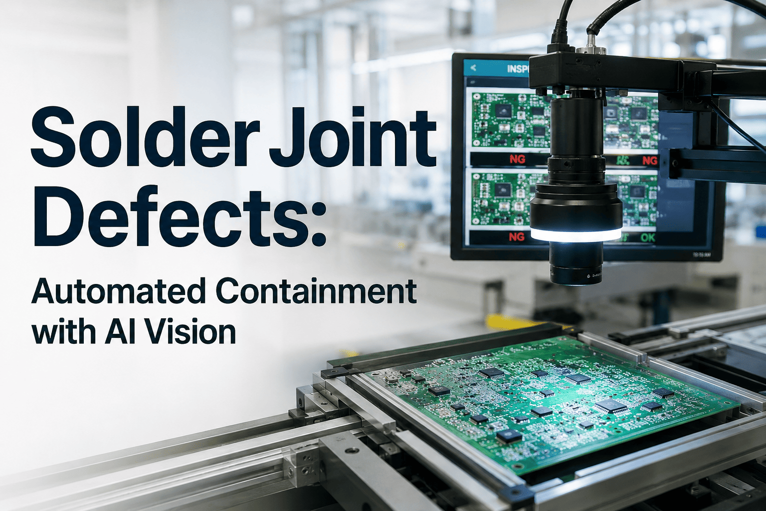
Solder joint defects kill PCB reliability at the interconnect level — a cold joint at a BGA ball, a void inside a QFN thermal pad, or a 0.3mm bridge between fine-pitch leads. By the time a field failure traces back to one, the defect has already propagated through hundreds of assemblies. The question is no longer whether AI vision can detect these — it is whether detection translates into containment: the line stops, affected boards divert to rework, and a QMS record with image, severity, and disposition exists before the next panel indexes.
Solder Joint Defects: Automated Containment with AI Vision
Deep-learning detection rates that manual inspection cannot sustain across shifts — wired directly into your PLC, MES, and QMS so every defect triggers a routing decision in milliseconds, not a spreadsheet entry at end of shift.
per frame, on-prem GPU
bridge, void, cold joints
on existing SMT line
with image + disposition
Understanding Solder Joint Defects
A solder joint is a metallurgical bond formed under a specific thermal profile. When that profile drifts — or when paste volume, stencil aperture, or component coplanarity fall outside their process window — the joint fails mechanically or electrically. Defects cluster predictably: BGA arrays hide voids under the package where no camera sees; QFN thermal pads trap gas; fine-pitch SOIC leads bridge when paste slumps; through-hole barrels cold-solder when preheat is insufficient.
Why Manual and Rule-Based Inspection Miss Them
A human inspector on hour six of a shift sees what they expect to see. Rule-based vision systems see what they are told to see — and break the moment a new component variant, a different solder paste lot, or a 15% shift in LED intensity arrives. Both approaches share a failure mode: they degrade silently. You discover the gap at final test, or worse, at a customer return.
Rule-based vision fails because it depends on fixed thresholds — edge contrast above 0.6, pad area within 5% of golden template. When the paste lot changes reflectivity, or a new LED bank ages yellow by 200 hours, those thresholds produce false accepts and false rejects simultaneously. Deep learning models learn the distribution of acceptable joints, not a single template, which is why they tolerate drift that breaks rule-based systems overnight.
Imaging Setup That Works
No model compensates for an image where the defect is not visible. Solder joints are specular metallic surfaces — they reflect light sources directly into the camera, creating blown highlights that hide the very features you need. The imaging architecture must make the defect legible at line speed, typically 0.5–1.2 seconds per board at standard AOI belt rates.
AI Model Training and Validation
A solder joint detection model is only as good as the label distribution it learns from. The most common failure is not architecture — it is class imbalance. A line producing 99.3% good joints yields 7 defective samples per 1,000 boards. Training a model on that natural distribution teaches it to predict "good" every time and still hit 99.3% accuracy. Useful models require deliberate defect mining and augmentation.
| Defect Class | Precision | Recall | False Reject | Min Samples Trained |
|---|---|---|---|---|
| Bridge / Short | 99.1% | 98.7% | 0.4% | 600 |
| Tombstone (0402/0201) | 98.8% | 98.2% | 0.6% | 500 |
| Insufficient Solder | 97.4% | 96.1% | 1.1% | 1,200 |
| Cold / Dull Joint | 96.2% | 94.8% | 1.8% | 1,500 |
| BGA Void (X-ray) | 97.9% | 96.5% | 0.9% | 800 |
| QFN Thermal Void (X-ray) | 95.6% | 93.2% | 2.1% | 1,000 |
Containment: Stop, Route, Record
Detection without containment is a dashboard. The value of AI vision on an SMT line is realized only when the inference result drives a physical routing decision — and that decision is logged in your QMS with the evidence attached. iFactory fires containment actions through Level 2 PLC/DCS integration in under 50 milliseconds from inference completion.
Root Cause Analysis from Production Data
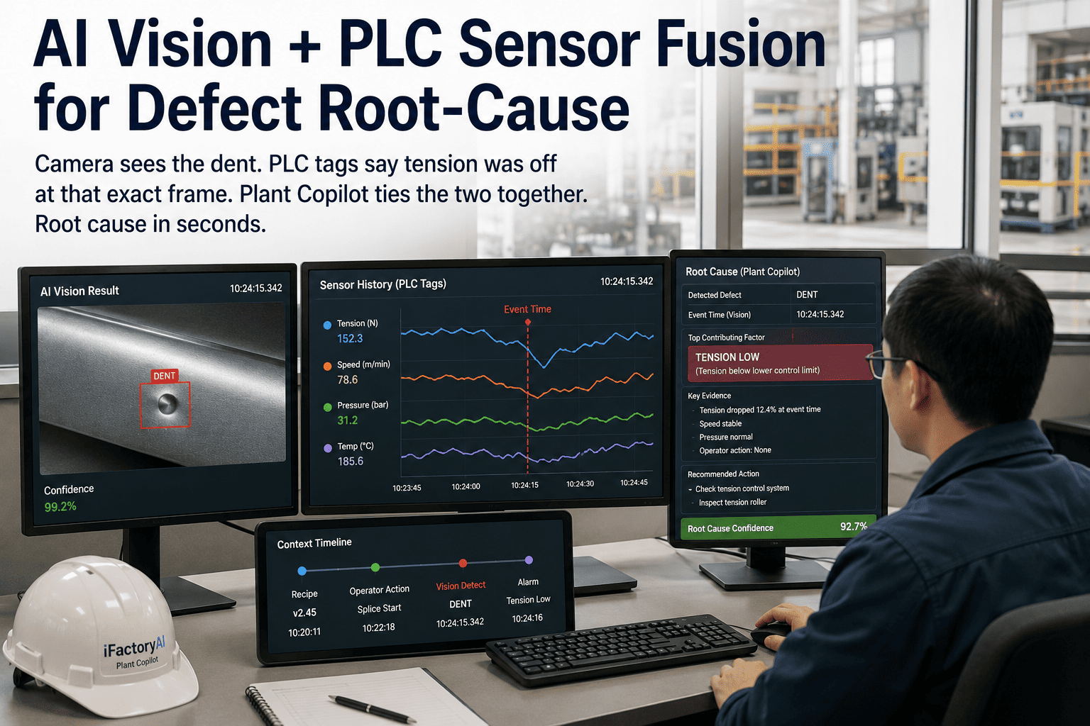
When a defect spikes, the question is not "what did the model find?" — it is "what changed on the line?" iFactory captures PLC tags at the exact moment of detection: reflow oven zone temperatures, paste printer squeegee pressure, placement head Z-force, ambient humidity. The result is a time-aligned correlation matrix that points at the process variable that drifted, not a guess.
Benchmarks and Pilot Scoping
A pilot is not a proof-of-concept demo. It is a scoped deployment on one line, one product family, with measurable containment outcomes. The goal is to validate detection rates on your boards, your defect distribution, your imaging conditions — and to wire the containment loop end-to-end before scaling to additional lines.
FAQ
Common questions from quality and process engineers evaluating AI vision for solder joint defect containment.
Send Your Boards. Get a Feasibility Read in 5 Days.
Ship 10–20 physical boards with confirmed solder joint defects, or share 500+ images from your AOI archive. Our engineers will validate imaging legibility, run a preliminary model evaluation, and return a report with expected detection rates and a containment integration plan — before you commit to a pilot.