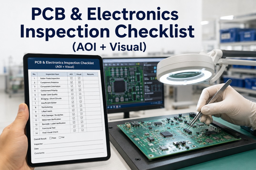
PCB defects are the leading cause of electronic assembly failure in the field — and the cost of a single undetected solder defect can exceed $10,000 in rework, recall, or liability by the time it reaches the customer. IPC-A-610J (2024) sets the global acceptance standard for assembled electronics, defining exactly what is acceptable, what is a process indicator, and what is a defect across three product classes. With automated optical inspection (AOI) achieving 98-99% defect detection at 5,000+ components per hour, no high-volume SMT line can rely on visual inspection alone. This PCB and electronics inspection checklist gives quality engineers, production supervisors, and electronics manufacturers a complete framework covering AOI setup, visual inspection criteria, solder joint acceptance, component placement verification, and IPC-A-610 class requirements — designed to reduce escapes, lower false call rates, and build a closed-loop quality system.
Unify AOI Exports and Manual PCB Inspection Data on a Single Quality Dashboard
iFactory's electronics inspection module ingests AOI machine data and merges it with manual visual inspection records — giving quality engineers a single view of every board. Flagged defects auto-generate corrective actions. Inspection records are retained for IPC-A-610 compliance audits. No more chasing AOI spreadsheets or paper inspection forms.
Where Inspection Fits in the SMT Assembly Line
A modern SMT line has four natural inspection gates. Each gate serves a different purpose: catching defects early (when they cost pennies to fix) vs. catching them after reflow (when rework dollars add up). A closed-loop inspection strategy uses data from each gate to feed back upstream — reducing defect generation rather than just sorting good boards from bad.
3D SPI measures paste height, volume, area, and offset before components are placed. Catches insufficient paste, bridging risk, and misaligned deposits at the source. Typical target: paste volume within 50-130% of stencil aperture.
Placed after pick-and-place, before reflow. Catches missing components, polarity errors, skew, and tombstoning while defects are still reworkable without desoldering. Fixing a misplaced component here takes seconds vs. minutes after reflow.
The primary quality gate. 3D AOI inspects every solder joint for bridging, insufficient solder, lifted leads, solder balls, and joint volume. True 3D systems measure absolute height and volume — capturing defects that 2D systems miss. Detection rate: 98-99%.
X-ray (AXI) for hidden joints under BGA, QFN, and LGA packages — detecting voids, head-in-pillow, and internal bridges. Final visual inspection per IPC-A-610 verifies cleanliness, conformal coating, mechanical assembly, and marking. Used together, AOI + AXI catch over 99% of defects.
IPC-A-610 Class System — Three Levels of Acceptance
IPC-A-610J defines acceptance criteria for three product classes. The same solder condition can be acceptable for Class 1 and defective for Class 3. Specifying the class on the purchase order, assembly drawing, and quality agreement before production starts is essential — ambiguity here is the leading cause of inspection disputes between OEMs and EMS providers.
General Electronic Products
Consumer electronics, simple gadgets, non-critical devices. Highest tolerance for cosmetic variation. Function is the primary requirement. Visual thresholds are most permissive.
- Side overhang: up to 50% of pad width
- End joint width: at least 50% of pad
- Heel fillet: not required
- Solder voids: more tolerance
Dedicated Service Products
Industrial controls, telecom, commercial electronics. Moderate tolerance with long-life expectations. Most EMS projects default here unless otherwise specified in the contract.
- Side overhang: up to 50% of pad width
- End joint width: at least 50% of pad
- Heel fillet: not required
- Side joint length: at least 50% of lead width
High-Performance Electronics
Medical, aerospace, defense, safety-critical systems. Very low tolerance for workmanship escapes. Defect boundaries tighten significantly. Evidence requirements rise at every inspection point.
- Side overhang: up to 25% of pad width only
- End joint width: at least 75% of pad
- Heel fillet: required and visible
- Side joint length: at least 75% of lead width
Common PCB Solder & Assembly Defects — Reference Guide
Most SMT defects originate in three process areas: solder paste printing, component placement, and reflow profiling. The table below maps each defect to its primary cause, detection method, and IPC classification risk. Detection difficulty ranges from easy (visible under standard magnification) to hard (requires X-ray or 3D AOI).
| Defect | Primary Cause | Detection | Difficulty | IPC Class Risk |
|---|---|---|---|---|
| Solder Bridge | Excess paste, fine-pitch spacing, placement pressure | AOI / Visual | Easy | Defect all classes |
| Cold Joint | Insufficient heat, oxidation, poor wetting | Visual / Microscope | Medium | Defect all classes |
| Head-in-Pillow | Reflow profile, BGA ball oxidation, paste slump | X-ray / AXI | Hard | Defect all classes |
| Tombstoning | Thermal imbalance, pad size mismatch, reflow profile | AOI / Visual | Easy | Defect all classes |
| Insufficient Solder | Stencil clogging, poor paste release, aperture design | 3D AOI / Visual | Medium | Defect all classes |
| Voiding | Outgassing, moisture, reprofile, flux activity | X-ray / AXI | Hard | Varies by class |
| Polarity Reversal | Pick-and-place programming, feeder error | AOI / Visual | Medium | Defect all classes |
| Lifted Lead | Z-axis misalignment, coplanarity, PCB warp | 3D AOI | Medium | Defect all classes |
Stop Chasing AOI Spreadsheets — Centralise Every PCB Inspection Record in One System
iFactory brings AOI machine data, manual visual inspection results, and corrective action tracking into a single platform. Quality engineers see defect trends by board type and station in real time. Inspectors complete IPC-A-610-aligned checklists on mobile devices with photo evidence. Audit-ready records are retained automatically.
PCB & Electronics Inspection Checklist — 30 Checkpoints
This checklist covers the six essential inspection areas for PCB assembly quality. Each checkpoint maps to IPC-A-610J acceptance criteria. Use this as your daily inspection framework — customise questions for your specific board types, component packages, and customer class requirements.
Solder Joint Quality
5 itemsComponent Placement & Orientation
5 itemsSolder Mask & PCB Surface Condition
5 itemsTrace Integrity & Pad Condition
5 itemsCleanliness, Coating & Foreign Object Debris
5 itemsMechanical Assembly & Documentation
5 itemsAOI vs. Manual Visual Inspection — Performance Benchmarks
The decision to invest in AOI is not about replacing inspectors — it is about deploying inspection resources where they add the most value. AOI handles high-speed, repetitive defect detection across thousands of components per board. Skilled inspectors focus on anomalies, grey-area judgments, and process improvement. The benchmarks below reflect published industry data from IPC-9716 and AOI manufacturer specifications.
Frequently Asked Questions
What is the difference between IPC-A-610 and J-STD-001?
IPC-A-610 is the acceptance standard for finished electronic assemblies — it defines what the completed product should look like. J-STD-001 is the process standard — it defines materials, methods, and soldering process requirements. They work together: J-STD-001 tells you how to build it, IPC-A-610 tells you what the finished result must look like. IPC-6012 covers bare board fabrication acceptance before assembly begins. Book a Demo to see how iFactory digitises IPC-A-610 inspection criteria.
What is a good false call rate for AOI?
A world-class AOI process targets a false call rate below 500 PPM (parts per million). Above 1,000 PPM, operators become desensitised and may begin auto-passing boards — allowing real defects to escape. A false call rate of zero is not desirable either; it indicates the sensitivity is too low and escapes are occurring. IPC-9716 (Requirements for AOI Process Control) provides detailed guidance on false call reduction methodology. 3D AOI systems typically achieve lower false call rates than 2D systems because height measurement eliminates ambiguous lighting-based judgments.
What are the IPC classes in PCB inspection?
IPC-A-610 defines three product classes: Class 1 (General Electronic Products) for consumer devices where function is the primary requirement; Class 2 (Dedicated Service Products) for industrial and telecom applications requiring extended life and reliable performance; and Class 3 (High-Performance Electronics) for medical, aerospace, and defense applications where equipment must function on demand in harsh environments. The same solder condition can be acceptable at Class 1, a process indicator at Class 2, and a defect at Class 3. Specifying the class on the purchase order before production starts is critical.
When should I use 3D AOI instead of 2D AOI?
Use 3D AOI when your boards include fine-pitch components (0201, 01005), BGA or QFN packages, components where lifted lead detection is critical, or when you need parametric measurement data for SPC. 3D AOI captures absolute height and volume measurements — enabling detection of lifted leads, coplanarity failures, and insufficient solder volume that 2D systems miss. The false call rate for 3D AOI is typically one-fifth that of 2D systems. For simple, large-component boards with generous tolerances, 2D AOI may be sufficient. Most high-volume SMT lines now default to 3D AOI for post-reflow inspection.
Can AOI replace manual visual inspection entirely?
No. AOI excels at high-speed, repeatable defect detection on visible surfaces — but it cannot inspect hidden joints (BGA, QFN), evaluate conformal coating quality, assess mechanical assembly feel, or make judgment calls on grey-area workmanship conditions. Manual visual inspection remains essential for first-article inspection, rework verification, low-volume/high-mix production, and Class 3 assemblies where inspector judgment is critical. The optimal approach is AOI for 100% inline inspection of all boards plus manual inspection for sampling, first articles, and anomaly resolution. iFactory gives you a single platform to manage both.
Digitise Your PCB Inspection Process — From AOI to Final Visual QC
iFactory gives electronics manufacturers a single platform for managing all PCB inspection data: AOI machine integration, IPC-A-610-aligned visual checklists, defect tracking, and real-time quality dashboards. Stop managing inspection with spreadsheets and paper forms. Get a complete, audit-ready picture of every board you ship.




-checklist-for-manufacturers.jpg)