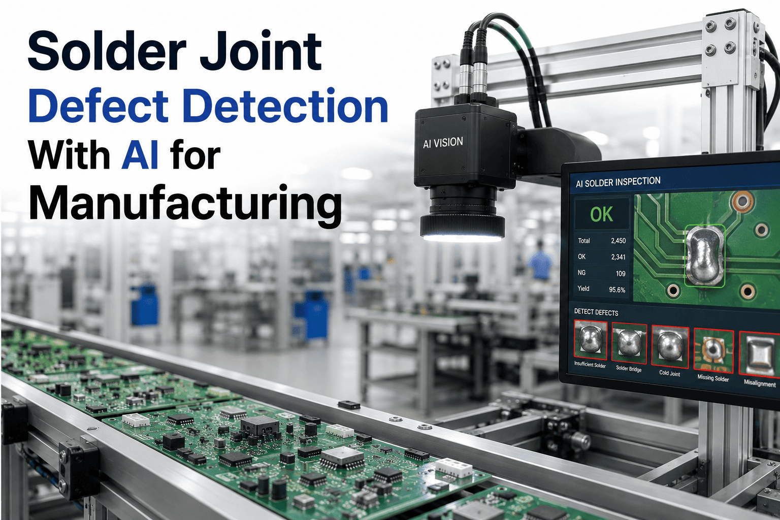
A cold joint and a good joint can differ by a few degrees of surface texture that a rule-based AOI camera reads as a pass and a trained eye reads as a five-second field failure waiting to happen. Solder joints are the most numerous failure point on any assembled board — a single PCB can carry hundreds to thousands of them, and every one is a potential open circuit or intermittent connection. Human inspectors are estimated to make visual inspection errors in 20 to 30 percent of cases, with accuracy varying by fatigue and defect type. AI changes what "inspection" means for a solder joint: instead of comparing against a fixed geometric template, a trained model evaluates fillet shape, wetting angle, and surface texture holistically, the way an experienced inspector does, but without the fatigue curve. To see what that looks like against your own board library, book a 30-minute walkthrough.
Every Solder Joint Is a Potential Failure Point. AI Catches the Ones Your AOI Misses.
Rule-based AOI checks joints against fixed geometry. AI vision learns what good and bad joints actually look like — fillet shape, wetting angle, surface texture — across your specific components and processes.
The Six Solder Defects That Cause the Most Field Failures
Solder defects aren't one problem — they're a family of distinct failure modes, each with a different visual signature, a different root cause on the line, and a different downstream risk if it escapes inspection. Recognizing which defect you're looking at is the first step to fixing the process that's producing it, not just rejecting the board. A missing-hole defect and a cold joint both fail final test, but they trace back to completely different upstream causes — etching versus reflow profile — and a taxonomy that treats them as interchangeable "solder problems" makes root-cause analysis slower than it needs to be.
Cold Joint
Incomplete reflow leaves the joint dull, granular, and rough instead of smooth and shiny. Mechanically weak and prone to cracking under thermal cycling or vibration — often invisible electrically until it fails in the field.
Solder Bridging
Excess solder forms an unintended connection between adjacent pads or pins, especially common on fine-pitch components. Creates a direct short circuit risk that can disable the board entirely.
Insufficient Solder
Inadequate joint volume leaves a fillet too thin to guarantee a reliable connection. Can pass initial electrical test yet carry elevated resistance or fail under mechanical stress later.
Tombstoning
Uneven wetting forces during reflow lift one end of a passive component off its pad, standing it on end like a tombstone. The joint on the lifted side is open, breaking the circuit entirely.
Head-in-Pillow
Under BGA packages, the solder ball and the paste fail to fully merge during reflow, leaving a visually plausible joint with a hidden non-wetted interface. Invisible to surface-only inspection.
Solder Voiding
Trapped gas or flux creates internal voids within the joint volume, weakening mechanical strength and thermal conductivity even when the visible surface looks acceptable.
Why Rule-Based AOI Struggles With Solder Specifically
Automated Optical Inspection has been the industry standard for decades, and it remains genuinely useful — but the technology's core limitation shows up most clearly on solder joints. Rule-based systems compare captured images against programmed geometric parameters: expected fillet height, expected reflectivity, expected shape within a defined tolerance window. Solder joints don't cooperate with that model nearly as well as component placement does, because acceptable joints carry far more natural visual variation than acceptable component positions do. Two joints can differ visibly in shape and still both be perfectly reliable, while a third joint that looks superficially similar to either one is quietly cold underneath — a distinction a fixed threshold has no way to make, because it was never built to reason about the joint as a whole, only to measure it against a single reference number.
The Inspection Pipeline: From Bare Board to Field-Ready
Solder joint quality isn't caught at a single checkpoint — it's monitored across several stages of the assembly process, each catching a different category of defect before the board moves any further downstream. Skipping a stage means the defects that stage would have caught only surface later, when the cost of finding them has multiplied.
Optical vs. X-Ray: Which Defects Each Method Can Actually See
Not every solder defect is visible from the surface, and understanding the physical limits of optical inspection is essential to specifying the right inspection strategy for a given board. A defect classification that mixes methods appropriately catches everything; one that relies on optical inspection alone leaves the hidden defect categories completely unmonitored — and those hidden categories are frequently the ones that cause the most expensive field failures, precisely because nobody was looking for them until the product had already shipped.
| Defect Type | Visible to 2D/3D AOI | Requires X-Ray (AXI) | Why |
|---|---|---|---|
| Cold joint | Yes | No | Surface texture and reflectivity are directly visible to optical cameras |
| Solder bridging | Yes | No | Bridge between adjacent pads is on the visible surface |
| Tombstoning | Yes | No | Component lift-off is a visible physical position defect |
| Head-in-pillow | No | Yes | Non-wetted interface hides beneath the BGA package body |
| Solder voiding | No | Yes | Internal gas or flux voids exist inside the joint volume, invisible from any surface angle |
| Hidden joint bridging | No | Yes | Joints under opaque packages cannot be reached by any camera, regardless of angle or lighting |
See Which Defect Categories Your Current AOI Is Actually Missing
iFactory maps your existing inspection coverage against the full solder defect taxonomy, then shows exactly where AI vision closes the gap — without replacing hardware you've already invested in.
A Composite Scenario: The Defect That Kept Escaping Final Test
An automotive electronics supplier producing a sensor control board had run its SMT line with rule-based AOI for years, with post-reflow inspection tuned to catch the obvious defects — bridging, missing components, gross insufficient solder. Field return rates on one specific board revision had crept upward over two quarters, and functional test at the end of the line wasn't catching the problem before shipment. The failure mode looked electrical and intermittent, the kind of issue that's notoriously hard to trace back to a specific manufacturing step, and the quality team had already spent several weeks chasing a component supplier lead that turned out to be a dead end.
The root cause turned out to be a subtle, recurring cold joint pattern on a particular fine-pitch connector, occurring on roughly one board in four hundred — frequent enough to matter at volume, rare enough that it had never triggered the AOI's fixed reflectivity threshold, which had been calibrated conservatively to avoid excessive false calls on a board with naturally reflective ENIG surface finish. The joints in question weren't obviously cold to a quick visual scan; they carried a texture variation subtle enough that the rule-based system's threshold consistently read them as passing.
An AI model trained on labeled examples from the plant's own historical AOI alarm records, verified by process engineers, learned to recognize the specific texture signature of that connector's cold joint pattern with far more sensitivity than the fixed threshold ever achieved — without a corresponding increase in false calls on the rest of the board, because the model evaluated the joint holistically rather than against a single reflectivity number. The defect rate on that connector, once isolated, traced back to a reflow oven zone running slightly cool on one specific thermal profile. Correcting the profile eliminated the defect at the source, and the AI inspection layer continued monitoring the connector afterward as a standing check against recurrence.
The Business Case: What Changes When Solder Inspection Gets Smarter
Solder defects sit at the most expensive point on the cost-of-quality curve for electronics manufacturing — catching one at post-reflow inspection costs a fraction of what the same defect costs once it escapes to functional test, and a small fraction of what it costs after it reaches a customer as a field failure. The value of AI-augmented solder inspection compounds specifically because it moves detection earlier and reduces the false calls that slow the line down in the meantime. The metrics below aren't abstractions — they map directly onto the scrap ledger, the warranty budget, and the line-throughput report that quality and operations leadership already review every month.
Combining AOI with complementary inspection stages has been shown to cut finished PCB failure rates by over 85% in production deployments.
Earlier detection of bridging, cold joints, and poor hole fill keeps defective boards from advancing further into assembly, cutting scrap costs by more than 90%.
The baseline error rate for manual visual inspection alone — the gap AI-augmented vision is specifically designed to close.
Electronics manufacturing accounts for the largest single-sector share of the global AI defect detection market, driven largely by solder and placement inspection.
Building a Solder Inspection Strategy: What to Match to What
The manufacturers who get the most out of AI solder inspection don't buy a generic solution and hope it covers everything — they know exactly which defects threaten their specific boards and match inspection strategy to those failure modes. Fine-pitch bridging risk, tombstoning-prone reflow profiles, and BGA head-in-pillow exposure each call for a different combination of inspection method and model training focus. The four steps below describe the sequence that separates a strategy genuinely built around a plant's real defect risk from a shrink-wrapped inspection package that happens to run on the same line.
Identify Your Highest-Risk Defect Categories
Pull historical AOI alarm and field return data to find which defect types actually drive your scrap and warranty costs — not a generic industry list, your specific pattern.
Match Inspection Method to Visibility
Confirm which of your risk categories are surface-visible and which require X-ray coverage for hidden joints beneath BGAs and other opaque packages.
Build the Training Dataset From Your Own Boards
The strongest models train on labeled images sourced from your own historical AOI alarm records, verified by your process engineers — not a generic public dataset.
Layer AI on Existing Hardware First
AI vision augments proven AOI and AXI hardware rather than replacing it — the strongest lines don't choose between AI and existing equipment, they combine both.
Frequently Asked Questions
The questions below reflect what process engineers and quality managers most often ask when evaluating a move from rule-based AOI to AI-augmented solder joint inspection.
Do we need to replace our existing AOI or AXI equipment to add AI inspection?
No — in most deployments, AI vision layers on top of the imaging hardware you already have rather than requiring a full equipment replacement. The AI model processes the same image data your AOI cameras already capture, applying a learned classifier instead of, or alongside, fixed geometric rules. Where new hardware does make sense is when existing cameras lack the resolution needed for a specific fine-pitch defect category. Book a 30-minute walkthrough to assess compatibility with your specific line.
How does AI reduce false calls compared to rule-based AOI?
Rule-based systems flag anything outside a fixed geometric or reflectivity threshold, which means natural, acceptable variation in joint appearance frequently trips the same alarm as a genuine defect. An AI model trained on a large set of labeled good and bad examples learns the fuller pattern of what acceptable variation actually looks like, evaluating the full image context rather than a single measurement against a hard threshold. This is what allows AI-augmented inspection to reduce false-call fatigue while simultaneously catching subtler true defects that rule-based thresholds miss.
Can AI vision catch defects hidden under BGA packages?
Not from optical imaging alone — no camera, however capable the underlying model, can see through an opaque component body. Defects like head-in-pillow, internal voiding, and hidden joint bridging beneath BGAs require X-ray inspection (AXI), because the physical limitation is optical, not algorithmic. AI models can and do process X-ray image data the same way they process optical images, so the AI layer extends to hidden joints once paired with X-ray hardware. Contact support to discuss AXI integration for your board mix.
How much training data do we need before an AI solder inspection model is reliable?
The most reliable models train on labeled datasets sourced from a plant's own historical AOI alarm records, manually verified by process engineers, rather than a generic public defect dataset. The exact volume needed depends on defect rarity — common defects like bridging need fewer labeled examples than rare ones like the specific cold joint pattern on a single connector type — but a working baseline model is typically achievable from several weeks of production history combined with manual verification of flagged images.
What's the biggest mistake manufacturers make when adopting AI solder inspection?
Buying a generic, one-size-fits-all AI vision package instead of matching inspection strategy to the specific defect categories that actually threaten their boards — fine-pitch bridging, tombstoning-prone reflow profiles, or BGA head-in-pillow exposure each call for different training focus and, in some cases, different hardware. The manufacturers who get the strongest results start by identifying their highest-risk defect categories from their own historical data, then build the inspection strategy around that. Visit support for guidance on scoping a strategy around your specific board library.
Stop Losing Boards to Defects Your Fixed Thresholds Were Never Tuned to Catch
iFactory trains AI inspection models on your own board history and layers them onto your existing AOI and AXI hardware, closing the gap between what rule-based thresholds catch and what actually reaches the field. Book a 30-minute walkthrough and we'll map your defect risk against your current inspection coverage.