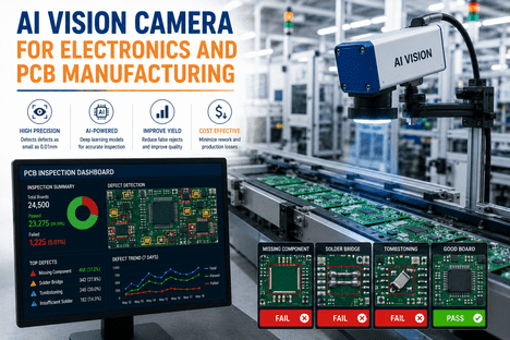
Electronics and printed circuit board manufacturing operates under quality demands that no other sector matches in density or precision. A single solder bridge, missing component, or tombstoned resistor on a PCB can cause device failure in the field — triggering costly recalls, warranty claims, and regulatory scrutiny. Conventional automated optical inspection systems have long been the industry standard, but first-generation AOI platforms struggle with the complexity of modern high-density boards, mixed-technology assemblies, and the sub-micron defect signatures that escape rule-based inspection logic. This is why electronics manufacturing now accounts for 34% of the global AI defect detection market — the largest share of any single sector — as manufacturers replace or augment legacy AOI with AI vision systems capable of learning defect patterns rather than merely checking against fixed templates. iFactory's AI Vision Camera platform delivers sub-micron solder inspection, missing component detection, bridging and tombstoning identification, and post-reflow quality verification at full line speed — with model accuracy that compounds as production data accumulates. Quality engineers, process managers, and procurement teams evaluating AI vision upgrades for their SMT, through-hole, or mixed-technology lines are encouraged to Book a Demo with iFactory to assess deployment performance against their current AOI false-call and escape rates.
Replace AOI False Calls with AI-Powered PCB Inspection That Learns Your Line
iFactory's AI Vision Camera detects solder defects, missing components, tombstoning, and bridging at sub-micron precision — on existing ONVIF infrastructure with NVIDIA edge processing.
AI Vision Camera for Electronics and PCB Manufacturing: Sub-Micron Inspection at Line Speed
A technical guide to how AI vision systems detect solder defects, missing components, tombstoning, and bridging on high-density PCBs — outperforming legacy AOI on false-call rates, escape rates, and adaptation to new board designs. Book a Demo to see iFactory's detection benchmarks on your board types.
Why First-Generation AOI Cannot Keep Pace with Modern PCB Complexity
Traditional automated optical inspection systems operate on rule-based logic — they compare a scanned board image against a programmed golden reference and flag deviations above a threshold. This approach works acceptably for simple, stable board designs with wide tolerances. It fails at scale when boards become more complex, component packages shrink, mixed-technology assemblies introduce varied solder joint geometries, and new product introductions require rapid reprogramming of inspection parameters. Rule-based AOI produces two failure modes that cost electronics manufacturers measurable quality and throughput losses: false calls that halt the line for non-defects, and genuine escapes where defect signatures fall below the static detection threshold. AI vision systems trained on real defect examples from your production process eliminate both failure modes by learning what actual defects look like — not just what a deviation from a template represents. iFactory closes this gap for electronics manufacturers by combining deep learning defect models with NVIDIA edge inference and existing camera infrastructure. Book a Demo to compare iFactory's false-call and escape rates against your current AOI system.
Solder Joint Defect Detection
AI vision identifies insufficient solder, cold joints, voids, bridging, and excess solder across all joint types — including BGA, QFN, and fine-pitch SMD — at sub-micron resolution without the reprogramming overhead of rule-based AOI systems.
Missing and Misplaced Components
Deep learning models verify component presence, orientation, and placement accuracy across all package types — detecting missing, rotated, flipped, and offset components that pass visual checks but fail functional test downstream.
Tombstoning and Bridging
Tombstoning — where one end of a passive component lifts during reflow — and solder bridging between adjacent pads are among the most common and costly SMT defect types. AI vision detects both in real time at post-reflow inspection stations.
Polarity and Orientation Errors
Polarized components — electrolytic capacitors, diodes, and ICs — placed with incorrect orientation pass solder inspection but cause functional failure. AI vision verifies polarity markings and orientation bands against the board's reference design at placement speed.
PCB Surface and Substrate Defects
Board-level defects — copper delamination, solder mask voids, via contamination, and surface oxidation — are detected before component placement, preventing defective substrate from proceeding through the full SMT process and accumulating rework costs.
Continuous Model Improvement
Unlike rule-based AOI that requires manual reprogramming for every new board design, iFactory's AI models learn from each production run — improving detection accuracy over time and adapting to new component packages without engineering intervention.
AI Vision vs. Legacy AOI: Performance Benchmarks for PCB Inspection
The measurable difference between rule-based automated optical inspection and AI vision inspection is visible across every quality and throughput metric that matters in electronics manufacturing.
| Inspection Metric | Legacy AOI (Rule-Based) | iFactory AI Vision Camera | Impact |
|---|---|---|---|
| Solder Defect Detection Rate | 78–85% on complex assemblies | 97–99.4% across all joint types | ~20% improvement in escape prevention |
| False Call Rate | 15–30% of flagged boards are non-defects | Under 3% false positive rate | 10x reduction in unnecessary line stops |
| New Board Design Setup | 4–12 hours of AOI reprogramming per design | Model adapts from first production sample set | 90% reduction in NPI inspection setup time |
| BGA and Fine-Pitch Inspection | Limited — requires X-ray for hidden joints | Visual anomaly detection on all accessible surfaces | Broader coverage without additional capital equipment |
| Defect Classification | Binary pass/fail with limited defect coding | Full defect type classification with image evidence per unit | Root cause traceability per board serial number |
| Integration with CMMS / MES | Manual export — delayed quality reporting | Automatic work order and quality record generation in real time | Immediate corrective action trigger per defect event |
Four Stages of AI Vision Inspection Across the PCB Production Process
Effective PCB quality inspection requires AI vision coverage at multiple stages of the production process — not just at end-of-line. iFactory's platform deploys across pre-reflow, post-reflow, and final assembly inspection points to catch defects at the lowest-cost correction stage rather than at functional test or field failure.
Pre-Placement Substrate Inspection
Before any component is placed, iFactory's AI Vision Camera scans incoming PCB substrates for copper delamination, solder mask defects, via contamination, oxidation, and dimensional accuracy. Boards that fail substrate inspection are removed before the full SMT process adds further value — preventing the compounding cost of reworking a populated, reflowed assembly on a defective substrate.
Post-Placement Pre-Reflow Inspection
After pick-and-place and before the reflow oven, the system verifies component presence, orientation, polarity, and placement accuracy across every component on the board. Missing, rotated, flipped, and offset components are flagged for correction before reflow — avoiding the significantly higher cost of reworking soldered assemblies. The AI model verifies each component against the board's bill of materials and reference placement data.
Post-Reflow Solder Joint Inspection
Following reflow, the AI Vision Camera performs comprehensive solder joint analysis — detecting insufficient solder, cold joints, solder voids, bridging between adjacent pads, tombstoning on passive components, and excess solder formation. Results are classified by defect type and severity, logged with timestamped image evidence, and linked to the board's serial number for full traceability. Boards requiring rework are automatically flagged in the MES or CMMS with defect location and classification pre-populated.
Final Assembly and Conformal Coating Verification
For assemblies requiring conformal coating, mechanical fastening, or connector seating, iFactory's AI Vision Camera verifies coating coverage completeness, identifies uncoated areas over critical components, and confirms connector and fastener seating at final assembly stations. This inspection stage closes the quality record for each board unit before it exits the production floor, creating a complete per-unit audit trail from substrate to finished assembly.
See iFactory AI Vision Inspect Your PCB Defect Types
iFactory deploys on your existing ONVIF camera infrastructure and delivers calibrated solder defect detection within days — no AOI replacement required. Connect to your MES or CMMS via standard API in the same deployment window.
Deploying AI Vision Alongside Existing AOI: No Replacement Required
Electronics manufacturers evaluating AI vision for PCB inspection frequently raise three deployment concerns: whether the system requires replacing existing AOI infrastructure, how long model calibration takes for new board designs, and whether production imagery leaves the facility. iFactory's platform addresses all three directly. The AI Vision Camera connects to ONVIF-compatible cameras already installed at inspection stations — including cameras integrated with existing AOI enclosures in many configurations — without requiring capital equipment replacement. All inference runs on NVIDIA edge processors within the production facility network; board imagery is never transmitted to external servers. For new board designs, iFactory's pre-trained solder defect library covers the core defect taxonomy from first production samples, with site-specific fine-tuning completed within the first production batch. This approach enables electronics manufacturers to achieve AI inspection accuracy within days rather than the weeks or months required by legacy AOI reprogramming workflows. Facilities running high-mix, low-volume production — where new board designs enter the line frequently — benefit most significantly from this rapid adaptation capability.
Frequently Asked Questions: AI Vision Camera for PCB and Electronics Manufacturing
Q: Can iFactory's AI Vision Camera replace our existing AOI system?
iFactory can deploy alongside existing AOI systems as an AI overlay that reduces false calls and improves escape detection, or as a standalone inspection solution on production lines where legacy AOI has been removed. The platform connects to existing ONVIF cameras, making it compatible with most current inspection station camera hardware without capital equipment replacement.
Q: What solder defect types does iFactory detect on PCBs?
iFactory's AI Vision Camera classifies insufficient solder, cold solder joints, solder bridging between pads, solder voids, excess solder, tombstoning on passive components, and solder balling — covering the full range of SMT solder defect types encountered in reflow and wave soldering processes across SMD, through-hole, and mixed-technology assemblies.
Q: How does the system handle high-mix production with frequent board design changes?
iFactory's AI models use a pre-trained industrial defect library as a foundation, with board-specific fine-tuning completed from first production sample sets — typically within a single production run. High-mix lines benefit significantly from this approach compared to legacy AOI, which requires 4–12 hours of manual reprogramming for each new board design introduction.
Q: Does board imagery leave the facility for cloud processing?
No — all AI inference runs on NVIDIA edge processors located within the production facility network. Board imagery, defect classifications, and quality records are processed and stored locally. No production data is transmitted to external servers, satisfying IP protection and data security requirements for electronics manufacturers with strict confidentiality obligations.
Q: How does iFactory integrate with our existing MES or CMMS?
iFactory integrates with major MES and CMMS platforms via standard REST API connectors — automatically generating quality records, defect classifications, and corrective action work orders linked to each board's serial number. Integration is typically completed within one to two weeks without disrupting production. Book a Demo to review integration compatibility with your current production systems stack.
Q: What is the ROI timeline for AI vision inspection in electronics manufacturing?
Most electronics manufacturers achieve positive ROI within 3–6 months, driven by reduction in escape-related field returns, elimination of false-call line stops, accelerated NPI inspection setup, and reduced functional test failure rates. In high-volume SMT production, a 1% improvement in first-pass yield on a high-value assembly typically recovers the full platform cost within weeks.
Deploy AI PCB Inspection That Learns Your Defects — Not Just Your Templates
iFactory's AI Vision Camera delivers sub-micron solder defect detection, missing component verification, and full per-board traceability — on your existing infrastructure, deployed in days, connected to your MES and CMMS from day one.