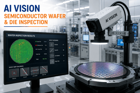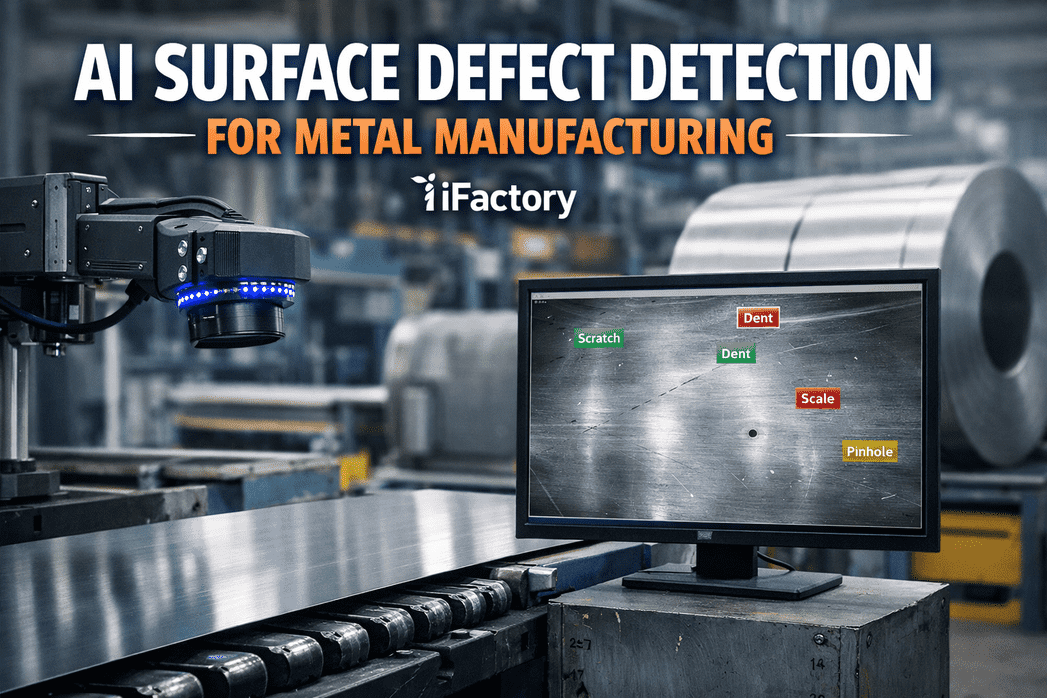
A single wafer moving through a modern fab carries enough value that a defect measuring less than a tenth of a micron, smaller than most bacteria, can render an entire die unusable and quietly erode a yield target that took months to hit. At the 5nm node and below, particles, scratches, pattern deviations, and overlay errors propagate through every subsequent layer once they slip past inspection, and traditional rule-based automated optical inspection systems only catch the defect types they were explicitly programmed to recognize. Undetected defects cost the global semiconductor industry more than $50 billion a year in yield loss, which is exactly the gap AI vision inspection was built to close by learning defect patterns instead of matching fixed rules. Fab quality teams evaluating whether their current inspection coverage still matches today's defect taxonomy can see the difference in classification accuracy directly by booking a short walkthrough of how the model performs against their own wafer images.
Catch the Defects Rule-Based AOI Was Never Programmed to See
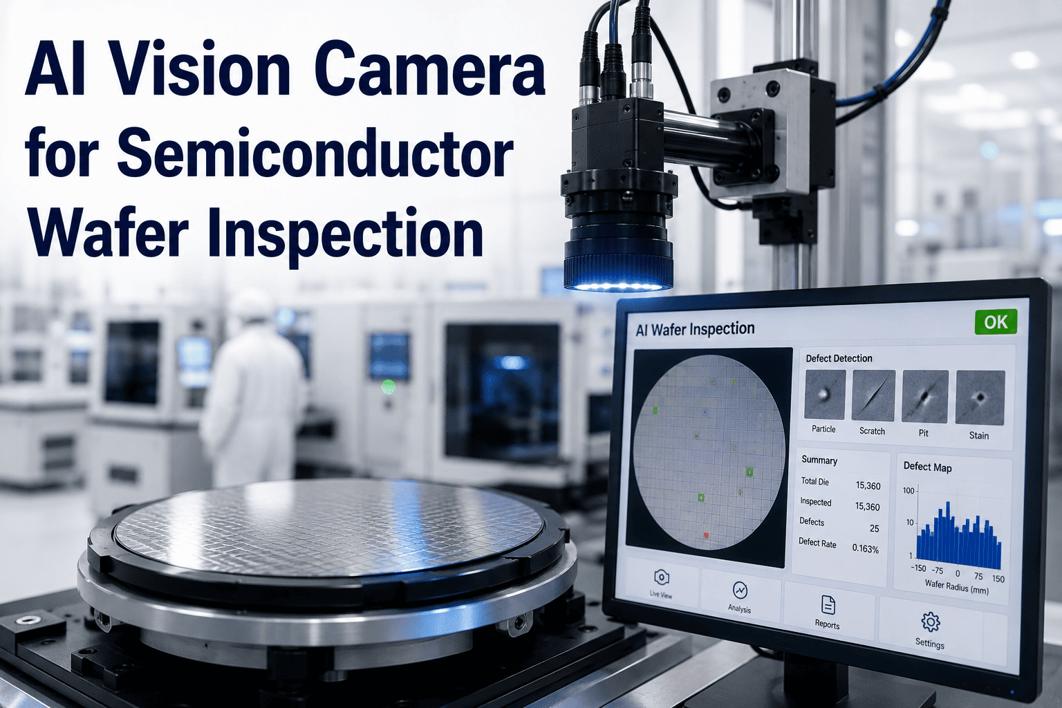
iFactory's AI Vision Camera inspects wafer surfaces for particles, scratches, pattern defects, and overlay errors at sub-micron resolution, running at full fab throughput without slowing the line.
What a Missed Defect Actually Costs a Fab
Yield economics at advanced nodes make inspection accuracy one of the highest-leverage investments a fab can make, because the payback math works out fast once a defect actually gets caught before it propagates.
Four Defect Classes AI Vision Is Trained to Separate
Wafer defects are not one problem, they are four different visual signatures with different root causes, and classifying each correctly is what determines whether engineering effort goes to the right fix.
Rule-Based AOI vs AI Vision Inspection
The gap between the two approaches is not incremental. It changes what a fab can rely on inspection data to do.
| Capability | Rule-Based AOI | AI Vision Inspection |
|---|---|---|
| Defect Classification Accuracy | Around 70% | Above 95% |
| New Defect Types | Requires manual rule programming | Learns from labeled examples continuously |
| Yield Rate Improvement | Limited to programmed defect list | 3-5% through early drift and pattern detection |
| Excursion Response Time | Often days, at end-of-lot electrical test | Hours, at the first affected wafer |
From Wafer Scan to Disposition in One Pass
Every wafer moves through the same detection sequence, converting a raw image into a classified, actionable defect map before the wafer leaves the inspection station.
See Your Own Wafer Images Classified
Bring a sample set of wafer images from your line and our team will walk through how the classification compares against your current AOI results.
Where the Return Actually Shows Up
AI vision inspection pays for itself through yield recovered and scrap avoided, not through inspection speed alone.
Frequently Asked Questions
Does AI vision inspection replace our existing AOI tools?
Not necessarily. Many fabs keep existing optical inspection hardware in place and replace the rule-based classification layer with a deep learning model trained on their own wafer images. The optics and imaging hardware often stay the same; what changes is the accuracy of what the system does with the image once it is captured, moving from around 70 percent classification accuracy on rule-based systems toward 95 percent or higher. The support team can review your current inspection hardware to confirm compatibility.
How does the model learn to classify new or unusual defect types?
Unlike rule-based systems that only catch defect types they were explicitly programmed to find, AI vision models learn defect patterns from labeled training examples and can generalize to visually similar but previously unseen anomalies. As new defect types appear on a line, engineers label a set of examples and the model incorporates them into its classification without requiring a full reprogramming cycle. This is particularly relevant at advanced nodes where the defect taxonomy keeps expanding faster than any fixed rule set can track.
Can this distinguish real defects from harmless process marks?
Yes, and this is one of the biggest practical advantages over rule-based inspection. Many wafers carry marks and patterns that are a normal part of the manufacturing process rather than a functional defect, and a rule-based system without adjustable thresholds tends to over-flag these as false positives. AI vision models trained on classified examples distinguish functional defects from normal process marks, and thresholds can be tuned to separate defects within tolerance from those that actually threaten yield.
How fast does this catch a yield excursion compared to waiting for electrical test?
Running AI-powered statistical process control on defect density per wafer, rather than waiting for end-of-lot electrical test, typically brings excursion detection down to hours instead of days. That difference matters directly in dollars: catching an excursion at the first affected wafer instead of after a full lot has moved through the line can be the difference between a small correction and $2 million or more of work-in-process value at risk.
What does it take to get this running on our line?
Implementation typically starts with a sample set of wafer images from your current inspection points to evaluate baseline classification performance against your existing AOI results. From there, the model trains on your specific defect taxonomy and process signatures rather than a generic dataset, since defect appearance varies meaningfully between process nodes and tool sets. Most fabs run a pilot on one inspection station before expanding line-wide, and a short call is the fastest way to scope that pilot for your line.
Protect Your Yield Target With Inspection That Learns
iFactory's AI Vision Camera brings sub-micron defect classification to wafer inspection, built for fab quality teams who cannot afford a missed excursion.