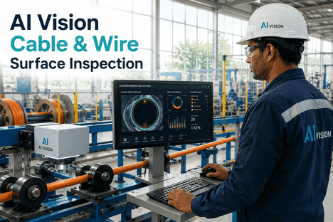
Semiconductor fabs now operate at the 5nm node and below, where a single particle smaller than 0.1 microns can render an entire die unusable and an undetected pattern deviation in photolithography propagates through every subsequent layer as a yield-destroying defect. Rule-based automated optical inspection — built on fixed threshold filters and golden-die comparisons — was adequate when defect geometries were large and predictable, but it cannot keep pace with the expanding defect taxonomy that advanced nodes generate. Undetected defects are estimated to cost the global semiconductor industry tens of billions of dollars annually in lost yield. iFactory's AI Vision Camera replaces fixed-rule recipes with deep learning models trained on wafer surface, edge, contamination, and packaging defect signatures — catching the categories that rule-based AOI consistently misses, at fab throughput speeds. Book a Demo to see classification accuracy on your specific wafer and die defect library.
Is Your AOI System Missing the Defects Hurting Your Yield?
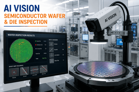
iFactory's AI Vision Camera detects sub-micron surface defects, pattern irregularities, and contamination signatures that rule-based inspection consistently misses at advanced nodes.
Why Rule-Based AOI Becomes the Bottleneck at Advanced Nodes
Traditional optical inspection compares each wafer image against a golden reference and flags deviations that cross a fixed threshold — an approach that worked reasonably well at older process geometries where defect types were limited and predictable. At 5nm, 3nm, and below, that model breaks down. New defect signatures appear with every node transition, and phenomena like EUV stochastic defects, line-edge roughness, and sub-resolution bridging do not conform to pre-written rules; they require a model that learns directly from imaging data. Industry benchmarks suggest that even a one-percentage-point improvement in defect detection accuracy can translate into a meaningfully larger yield gain, which is why the accuracy gap between rule-based AOI and AI vision on complex defect categories represents a fundamental shift in yield economics rather than a marginal improvement.
Wafer Surface Defects
Scratches, pits, crystal-originated pits, and stacking faults occur at scales from tens of nanometers to several microns. AI vision models trained on dark-field and bright-field imaging classify each by type, size, and location.
Edge & Pattern Irregularities
Line-edge roughness, bridging between adjacent features, and pattern shift grow more common as feature pitch shrinks. AI vision distinguishes real defects from process-normal variation without per-layer rule updates.
Particle & Contamination Signatures
Process chemicals, photoresist residue, and metal-ion deposition drive random yield loss. AI vision separates yield-killing particle types from benign residue that would otherwise consume review capacity.
Die & Packaging Anomalies
Die bond placement, solder bump coplanarity, and wire bond geometry require micron-level tolerance checks at high-speed bonding lines, across flip-chip, wafer-level, and 3D IC packaging formats.
How AI Vision Tracks a Wafer From Entry to Yield Pareto
Effective defect detection in a fab is not a single inspection step — it is a continuous workflow that captures defect signatures at every process transition where yield-limiting events occur. iFactory's AI Vision Camera integrates at each control point and builds a structured defect record per wafer that feeds the yield management workflow and the process engineering team's response process.
Incoming Wafer Baseline Inspection
Before any process step, AI vision establishes a baseline of the incoming wafer surface — capturing pre-existing scratch maps and edge defects so they are not mistakenly attributed to downstream process steps.
In-Line Process Step Inspection
Inspection immediately after lithography, etch, and CMP catches resist bridging, pattern collapse, and scratch clusters before a defect propagates into a permanent structural failure at the next layer.
Defect Classification & Pareto Generation
Every detected defect is classified by type, size, and wafer location, producing a ranked Pareto of yield-limiting defect types — generated within minutes rather than the days a manual review workflow typically takes.
Spatial Mapping & Tool Correlation
Defect location on the wafer carries systematic signatures — a ring pattern near the edge can point to a clamp or spin coater condition, while a column pattern can point to reticle contamination. Spatial AI mapping correlates the pattern against tool history automatically.
Excursion Alerting & Lot Disposition
When defect density on a wafer or lot crosses a statistical control threshold, an automatic excursion alert holds the affected lot for engineering review before it advances — preventing one process drift event from propagating through a full lot's worth of work-in-process inventory. Book a Demo to see this excursion workflow on your own defect library.
What Makes iFactory's AI Vision Built for Semiconductor Lines
iFactory's AI Vision Camera is not a generic machine vision toolkit retrofitted to wafer inspection — it is built around the imaging constraints, defect taxonomies, and integration requirements specific to semiconductor and advanced electronics manufacturing.
Four Capabilities That Set This Platform Apart
Inference runs on GPU-enabled compute co-located with the inspection station, keeping wafer image data on-premises and removing cloud latency as a constraint on wafer-per-minute inspection rates.
When a novel defect type appears from a process change or new material, the model retrains on a small set of labeled examples — cutting new-node inspection readiness from weeks of recipe engineering to days.
iFactory connects to yield management systems, MES platforms, and CMMS through standard protocols — a flagged defect cluster can automatically update lot history and open a maintenance work order.
Confirmed defects, reviewed false positives, and novel anomalies all feed back into the model through an active learning loop, so classification accuracy keeps improving as production data accumulates.
What This Means for Fab Yield Management
Improving defect detection accuracy at advanced nodes is not a quality-assurance line item — it is a direct lever on fab profitability. Fabs that move from rule-based AOI to AI vision recover yield that was previously being absorbed silently, one misclassified defect at a time.
Unsupervised anomaly scoring flags defect types the model has never seen before, routing them for engineering review instead of letting them slip past a fixed-rule recipe undetected.
High nuisance rates from aggressive AOI sensitivity settings bury real excursions in review queues. AI anomaly scoring keeps the false positive rate low enough that genuine defects surface quickly.
Automated spatial defect mapping against tool ID and process history replaces manual engineering analysis, shortening the path from defect detection to corrective action.
Few-shot retraining on new defect categories replaces multi-week recipe engineering cycles, helping fabs reach production-grade inspection readiness faster on each new process generation.
Statistical process control on defect density per wafer catches drift at the first affected wafer rather than at end-of-lot electrical test, protecting work-in-process inventory value.
A reliable, fully classified defect Pareto directs process improvement effort accurately, rather than chasing root causes implied by an inaccurate or incomplete defect breakdown.
Start a Turnkey AI Vision Pilot on Your Fab Line
iFactory's AI Vision Camera deploys on your existing inspection infrastructure with pre-trained models for wafer surface, edge, contamination, and packaging defects — integrated with your YMS and CMMS from day one.
Defect Detection Is a Yield Lever, Not a QA Checkbox
At advanced semiconductor nodes, defect detection accuracy is one of the most direct levers a fab has over its own profitability. The yield loss from undetected defects is not a fixed cost of manufacturing at small geometries — it is largely recoverable, concentrated in defect categories that AI vision detects and rule-based AOI consistently misses. iFactory's AI Vision Camera brings in-line process inspection, deep learning classification, spatial defect mapping, and SPC-integrated excursion alerting into one workflow that connects directly to your existing YMS and CMMS infrastructure. Book a Demo to see how this framework maps to your specific defect library and process layers.
AI Vision Wafer & Die Inspection — Common Questions Answered
What size of defects can AI vision detect on a wafer?
With high-resolution optical imaging and scatterometry correlation, the platform targets sub-micron surface particles and contamination, while pattern defects such as line-edge roughness and bridging at fine feature pitch are classified using SEM-correlated optical data for defect types that standard optical AOI alone cannot resolve.
How does the model handle a defect type it has never seen before?
Novel defect signatures are flagged by an anomaly detection layer that scores each image against the statistical distribution of known patterns, routing unfamiliar cases to engineering review. Once classified, those examples retrain the model using few-shot learning, typically within a day or two.
Can this integrate with our existing yield management and CMMS systems?
Yes — iFactory connects to yield management systems, MES platforms, and CMMS through standard protocols, reading the active lot recipe to apply the correct inspection model and writing defect classifications and SPC signals back in real time, including automatic work order generation when a defect pattern correlates with a specific tool.
What yield improvement is realistic from deploying AI vision inspection?
Documented deployments report meaningful yield rate improvement from earlier process drift detection alone, before accounting for the additional value of excursion containment and reduced false-positive review burden. The specific improvement depends on your current defect escape rate and the share of yield-limiting defects outside your existing AOI recipe's detection range.
How long does deployment take on an existing inspection line?
Integration with existing inspection tool data streams is typically completed over several weeks without interrupting production, with initial model training drawing on existing labeled defect archives. Packaging inspection lines with simpler defect taxonomies can reach production-grade deployment faster.